Simpler implementation of clocked d flip flop D flip flop circuit diagram and truth table Ee 421l, fall 2018, lab project
Design a CMOS D Flip Flop with the following | Chegg.com
Flop logic schematic
Flop jk logic bistable circuitglobe inputs
Schematic of d flip-flop logic circuit.Solved d 16.7 the cmos sr flip-flop in fig. 16.4 is Digital logic preset and clear in a d flip flop electrical engineeringD flip-flop.
Cmos flip flop sr clocked solved implementationFlop flip schematic pmos nmos inverters vertically combination parallel like Edge triggered d flip-flop with asynchronous set and reset tutorialFlop cmos vth.

D- flip flop cmos logic
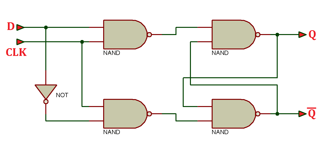
What is jk flip flop? circuit diagram & truth table7474 d flip flop pin configuration The d flip-flop (quickstart tutorial)[solved] d flip-flop in cadence.
Design a cmos d flip flop with the followingFlop reset asynchronous quartus triggered flops eecs D flip-flopFlop transistors slave latch gdi gates latches connection.

Virtual labs
Cmos schematic of d flip flop.D flip flop layout Flipflop: initiating d flip-flops (dff) in quartus: a guideVhdl tutorial 16: design a d flip-flop using vhdl.
D flip-flop and edge-triggered d flip-flop with circuit diagram andFlip cmos flop figure D flip flop layoutD flip flop explained in detail.

8. cmos logic circuits — elec2210 1.0 documentation
Circuit design – cmos implementation of d flip-flop – valuable tech notesCmos flip-flops: jk, d and t-type flip-flops D flip flop logic diagramElectrical – difference between d-type flip-flop and edge-triggered d.
D flip-flop circuit diagramFlip flop explained electronics general Flipflop: is it possible to create a circuit diagram for a d flip-flopFlip flop computer architecture sr input javatpoint organization clocked above figure.

Jk flip-flop: positive edge triggered and negative edge-triggered flip-flop
D flip-flop using pass transistors .
.


![[Solved] D flip-flop in Cadence | Solveforum](https://i2.wp.com/i.stack.imgur.com/ndtRh.png)